
Empowering minds, fueling futures.
Immersive courses. Engaged faculty. Inspired scholars. These are the heart of Miami University’s diverse arts and science curriculum. The College of Arts and Science (CAS) fosters a climate that promotes intellectual discovery and personal development through the 60+ undergraduate majors, dozens of minors, and 40+ graduate degree programs. Whatever your passion, CAS will equip you to obtain a great career that enables you to live your dreams, enact meaningful change, and become the person you desire to be.
Why Arts and Science?
At Miami University's College of Arts and Science, you’ll get a broad and diverse education that offers the "best of both worlds" — opportunities and resources typically found at much larger universities in a more intimate, personalized, interactive environment. You’ll gain critical thinking and communication skills through our rich diversity of rigorous academic opportunities and experiences. You'll cultivate intellect and creativity as we work toward the common good. And you'll develop the key building blocks to a happy, successful career in our ever-changing, globally minded workforce.

Upcoming Events in CAS
Pursue Transformative Experiences. Prepare for a Fulfilling Career.

Do More ...
As an undergraduate in the College of Arts and Science, you will get the personal attention and resources other universities reserve for their graduate students.
Our professors will encourage you to take an active role in their research teams, where you'll make real contributions and learn valuable skills. You may even present the results of your research at major conferences and see your work published in scholarly journals. These pre-professional experiences will give you a strong advantage for professional or graduate school acceptance as well as rich and rewarding careers.
ADMISSION QUICK LINKS

See More ...
Real-world experience doesn’t happen in just any classroom. You have to see the pressing issues firsthand before you can make solid contributions.
Across a variety of CAS research centers, you will have opportunities to work side-by-side with professors, community leaders, and industry experts to help actually implement solutions to today’s pressing issues. And our popular “Inside” study away workshops in Hollywood, Washington, New York, London, and more will take you behind the scenes in close contact with successful Miami alumni.
QUICK LINKS

Be More ...
Whatever your passion, customize your education to match your vision. Add a second major or a co-major. Explore a minor or two. It’s your education. We’re just the guide on your path to success.
Our expert academic advising staff and professors will work with you to achieve the goals that are uniquely you. We will help you navigate your chosen career field and academic interests via 11 CAS theme areas and nine overall career clusters where you focus on your professional interests while exploring similar careers within broad industry categories.
Meet Some of our Accomplished Students

Jack Bernacki '24
Political Science and Statistics

Jillian Schwab '24
Anthropology

Stella Lukusa '24
LSAMP, Biology, Mallory-Wilson Center for Healthcare Education

Ava Kalina '24
Political Science and Statistics
Where Passion and Talent Create Change and Opportunity
Discover why arts and science graduates are sought by top employers.
1 in 3
undergraduates doing research in experiential environments alongside leading faculty
98.4%
of May 2022 graduates are employed or enrolled in graduate school by fall
93%
of 2021-22 senior Miami applicants were accepted to law school (compared to 80% national average for the same period).
60.4%
of first-time applicants were accepted into medical school; around 20% higher than national average
Meet Our Teacher-Scholars
David Berg
University Distinguished Professor
Biology
College of Arts and Science
"In biology at Miami, we engage students in the classroom, in the laboratory, and in the field. Our undergraduates have the rare opportunity to conduct novel and timely research under the guidance of talented graduate students and passionate faculty. Our research on freshwater invertebrates both guides and supports conservation actions by numerous state and federal agencies."
Rodney Coates
Professor
Global and Intercultural Studies
College of Arts of Science
"As a teacher-scholar, I actively engage my students in research, knowledge production, and critical reflection. Miami University encourages excellence in its students and its faculty. It is a place where the teacher-scholar model becomes how we foster critical inquiry and maximize student achievement. At Miami, it is not through indoctrination and memorization, but student engagement and scholarship by which learning is accomplished."
Steven Conn
W.E. Smith Professor
History
College of Arts and Science
"What I most enjoy about teaching at Miami is the extent to which I am able to experiment with new methods and to try out new ideas with students who are keen to try new things too. I have the flexibility to explore things that I think students will find interesting or which are driving my own scholarly interests at a given moment. I think my scholarship has enriched my teaching but I know beyond a doubt that teaching Miami students has enriched my scholarship."
Renate Crawford
Adjunct Professor
Physics
College of Arts of Science
"The teacher-scholar model enables me to lift complicated concepts out of the textbook and show real-world examples to reinforce the underlying physics. Students are introduced to contemporary translational and applied research as they learn the basic principles of physics. Faculty at Miami are both teachers and scholars, transforming their classrooms through research, creating a vibrant teaching and learning environment, introducing students to what researchers and scholars are thinking about in their disciplines."
Cameron Hay-Rollins
Chair and Professor
Anthropology
College of Arts and Science
"Research is an adventure. As an anthropologist, I seek to understand how people cope with suffering, illness, and inequity. Whether in Indonesia, India, or Indiana, I venture into the unknowns of research to find evidence of how we might promote resilience, well-being, and equity in the most vulnerable moments of people’s lives. Research is an exciting activity, and Miami’s teacher-scholar model allows me to invite students into scholarly conversations and the surprising joy of pursuing research adventures."
Emily Legg
Associate Professor
English
College of Arts and Science
"As faculty, it is so invigorating to find that Miami students are reflective and active participants in their learning experiences, rather than just sitting back and passively consuming the materials I’ve provided. Together, we all strive to create a knowledge-making community in the classroom, where I find myself both teaching and constantly learning from students in ways that grows my own scholarship. By challenging ourselves to become better teacher-scholars, we all can create spaces where community knowledge can happen and inclusive teaching begins."
Wayne Nirode
Assistant Professor
Math
College of Arts and Science
“When I began thinking about leaving high school for the next phase of my professional career, it was important for me to go to a university that valued both teaching and research. To me, this is at the heart of the teacher-scholar model. After being at Miami University for six years, I do not think that I could have found a university that better aligns with my views on teaching and researching — in short the teacher-scholar model. I am proud to say that Miami is my professional home.”
Arnold Olszewski
Associate Professor
Speech Pathology and Audiology
College of Arts and Science
"As an instructor, my goal is to help future speech-language pathologists develop assessment and intervention plans using evidence-based methods. As a researcher, my goal is to work with students to develop, evaluate, and revise techniques for teaching early literacy skills. What I love about Miami is the strong emphasis on both teaching and research. Many schools prioritize one over the other, but I believe these go hand-in-hand. My favorite thing is getting a student who is scared of research to develop their own project and see the excitement they feel when they get their results."
Rosemary Pennington
Associate Professor, Journalism Area Coordinator
Media, Journalism, and Film
College of Arts and Science
Vaishali Raval
Professor
Psychology
College of Arts and Science
Elizabeth Wardle
Roger and Joyce Howe Distinguished Professor of Written Communication and Director
English, Howe Center for Writing Excellence
Ellen Yezierski
Professor and Director
Chemistry and Biochemistry, Center for Teaching Excellence
College of Arts and Science
The College of Arts and Science
Representing nearly half of all students, the College of Arts and Science (CAS) is Miami University's largest division and the centerpiece of liberal arts — the wide range of subjects in the natural sciences, social sciences, and humanities crucial for the development of key professional skills desired by employers.

Contact Us
100 Bishop Circle
143 Upham Hall
Miami University
Oxford, Ohio 45056
CAS@MiamiOH.edu
513-529-1234
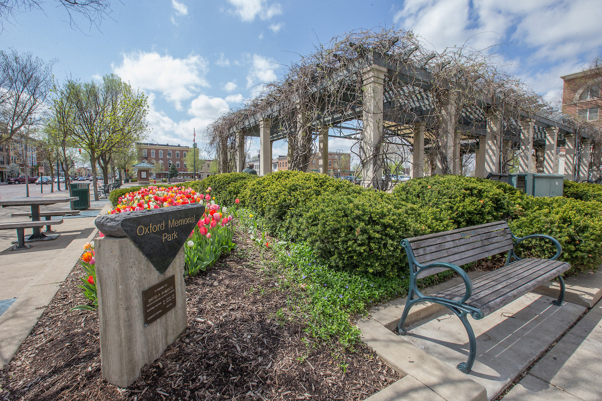
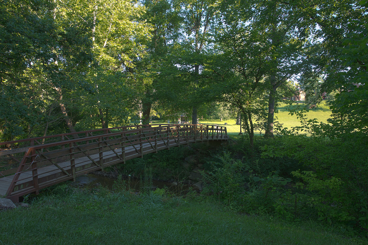
Visit
There’s a lot to say about one of America’s most beautiful campuses. Find out why so many choose Miami for their most memorable years.
Apply
The big question is, “Where will you go after college?” With a degree from Miami University, the answer is, “Wherever you want.”